DC-DC Conversion Without Inductors
Abstract: Charge pumps are often the best choice for powering an application that requires both low power and low cost. This application note discusses integrated charge pumps and explains how to calculate power dissipation in a charge pump.
A familiar problem in system engineering is the subsystem whose power requirements are not met by the main supply. In such cases, the available supply rails are not directly usable, nor is the direct use of battery voltage (when available) always an option. Lack of space can prevent inclusion of the optimal number of cells, or the declining voltage of a discharging battery may not be acceptable for the application.
Voltage converters can generate the desired voltage levels, and charge pumps are often the best choice for applications requiring some combination of low power, simplicity, and low cost. Charge pumps are easy to use, because they require no expensive inductors or additional semiconductors.
Charge-pump voltage converters use ceramic or electrolytic capacitors to store and transfer energy. Although capacitors are more common and much cheaper than the coils used in other types of DC-DC converters, capacitors cannot change their voltage level abruptly. A changing capacitor voltage always follows the exponential function, which imposes limitations that inductive voltage converters can avoid. Inductive voltage converters are, however, more expensive.
Capacitive voltage conversion is achieved by switching a capacitor periodically. Passive diodes can perform this switching function in the simplest cases, if an alternating voltage is available. Otherwise, DC voltage levels require the use of active switches, which first charge the capacitor by connecting it across a voltage source and then connect it to the output in a way that produces a different voltage level.
A common integrated circuit using this principle is the ICL7660, which some consider the prototype of the classic charge pump. The ICL7660 integrates switches and the oscillator so that the switches S1, S3 and S2, S4 work alternately (Figure 1). The configuration shown here inverts the input voltage. With a slight change in the external connections, it can double or divide the input voltage as well.
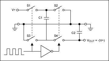
Figure 1. These essential components illustrate the mechanics of charge-pump operation.
Closing S1 and S3 charges the flying capacitor, C1, to V+ in the first half cycle. In the second half, S1 and S3 open and S2 and S4 close. This action connects the positive terminal of C1 to ground and connects the negative terminal to VOUT. C1 is then in parallel with the reservoir capacitor C2. If the voltage across C2 is smaller than that across C1, charge flows from C1 to C2 until the voltage across C2 reaches -(V+).
An integrated fixed-frequency oscillator drives the periodic switching. This circuit has no output regulation, and the switching frequency remains constant for all loads. Thus, the output-voltage variation depends strongly on the load. With no load, the output voltage corresponds to the negative input voltage: VOUT = -(V+). As the load increases, VOUT decreases. Output current for the ICL7660 is, therefore, limited to about 10mA. This is partly due to its low oscillator frequency, and partly due to its integrated analog switches which are far from ideal. These switches in the "on" state exhibit several ohms of on-resistance. A detailed calculation of the resulting power dissipation will be shown later.
Pin-compatible circuits (MAX660, MAX860/MAX861, MAX1680/MAX1681) feature higher switching frequencies and lower on-resistance in the switches. Because their switching frequencies are higher, these charge pumps operate with smaller capacitors and deliver higher output current. All the devices can be configured as a voltage inverter, doubler, or divider.
The MAX828/MAX829 and MAX870/MAX871, which were designed for inverter applications, reduce the required board area with a smaller package (SOT23) and smaller external capacitors. Pin-compatible versions of these devices (MAX1719/MAX1720/MAX1721) provide an additional shutdown pin for switching off the circuit. In that condition, the supply current drops to 1nA, the output disconnects from the input, and the output voltage drops to zero.
Consider a circuit designed to divide the input voltage by two and double the output current. It offers advantages over linear regulators (which usually convert power into heat), and benefits applications that require a limited output current. A 4mA to 20mA interface, for example, often provides a relatively high output voltage but a limited preset output current. Other applications include the many op amps and microcontrollers that now operate with very low supply voltages. In those circuits, dividing the supply voltage by two theoretically divides the power consumption by four.
The configuration of Figure 2 generates a regulated VOUT (= VIN/2) using the capacitive voltage divider C3, C4 and C5, C6. By switching the flying capacitor, C2, alternately between upper and lower halves of this divider, the IC counterbalances any load-dependant voltage differences. The circuit's switching frequency is 35kHz and its quiescent current is only 36µA. When load currents exceed 1mA, the circuit's efficiency exceeds 90%. Given very small load currents (i.e., below 100µA), however, even this low 36mA quiescent current reduces conversion efficiency. This switched-capacitor configuration provides both better regulation than a simple resistive voltage-divider, and higher efficiency than that obtained from a simple combination of a voltage-divider and an op-amp buffer. The IC specification limits VIN to 5.5V maximum.
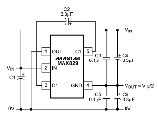
Figure 2. With the connections shown, this inverting charge-pump IC divides the input voltage by two.
Consider now a simple model in which a capacitor, C1, switches between the output voltage and V+ at frequency f (Figure 3). This model enables a discussion of charge-pump power dissipation.
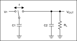
Figure 3. This model of a switched capacitor shows that it behaves like a resistor.
A reservoir capacitor, C2, and load, RL, are connected to VOUT. The charge transmitted per cycle is:
ΔQ = C1(V+ - VOUT)
Which produces a current, I, that depends on the frequency f:
I = fΔQ = fC1(V+ - VOUT).
After changing the equation according to Ohm's Law, an equivalent resistance, RERS, for the switched capacitor can be calculated as:
RERS = 1/fC1
This equation shows that the resistance and, consequently, the resistive losses decrease with increasing frequency and higher capacitance. Higher capacitance lowers the output resistance only until the switches' resistance and the capacitors' equivalent series resistance (ESR) exceed RERS. This internal loss (switching loss) can be reduced only by choosing low-ESR capacitors. Switch on-resistance can be lowered through the use of sophisticated new charge pumps.
Switching loss is caused by the voltage difference between the flying capacitor and the output capacitor, as well as by on-resistance in the switches. This voltage difference appears across the switches, causing dissipation in the application. As shown before, a switched capacitor behaves like a resistance. Thus, you can reduce output resistance and increase the output power by connecting several switched-capacitor devices in parallel.
Integrated charge pumps that regulate the output voltage operate without inductors. They offer regulated output voltages (e.g., 5V) and several power-saving modes. Devices such as the MAX682/MAX683/MAX684 regulated upconverters operate either in the efficient skip mode or in a fixed-frequency mode with reduced output ripple.
When a drop in output voltage is sensed by the internal comparator, the power-saving skip mode avoids unnecessary switching by activating only the internal oscillator. The result is lower quiescent current and lower switching dissipation, especially for light loads. Skip mode is preferable for low-power applications, because higher levels of quiescent current reduce overall efficiency.
To minimize output ripple, the circuit can oscillate in a fixed-frequency mode that is regulated between 50kHz and 2MHz. Regulation ensures that the flying capacitor is charged through an internal MOSFET with a charging current that depends on the load. A decreasing output voltage, caused by increasing power consumption, charges the capacitor with more energy. As benefits of the fixed-frequency mode, the output ripple is lower and the external components are smaller. If you have the impression that charge pumps provide only low output currents of a few milliamps, you will be surprised to learn that the MAX682 delivers as much as 250mA from a 5V output.
An improved design for maintaining a switching frequency that is constant and independent of the input voltage is shown in Figure 4.
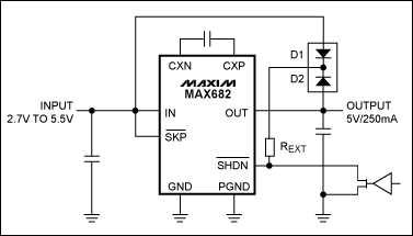
Figure 4. This regulated charge pump maintains a constant switching frequency.
The IC's internal switching frequency is controlled with current into its shutdown pin. The governing equation is taken from the device's data sheet:
REXT = 45000(VIN - 0.69V)/fOSC, with REXT in kΩ and fOSC in kHz
Normally, you calculate the value of the external shutdown resistor with the given input voltage and the desired switching frequency. In this case, however, the equation shows that switching frequency and current in the shutdown pin depend on the input voltage, VIN. If the input voltage varies, the switching frequency varies too.
Two diodes direct current into the shutdown pin. D1 ensures a reliable startup by directing current from the input to the shutdown pin when the supply voltage is first turned on. When the output voltage achieves 5V or rises higher than VIN, the switching frequency becomes constant because D2 conducts current from the stable output voltage. A tiny diode array in a 3-pin SOT23 package (BAV70) is recommended for the D1-D2 combination. Note that a shutdown function is still available. Driving the shutdown pin to ground with an open-drain MOSFET simply short circuits the preset-frequency current to ground.
Many applications need an additional negative voltage such as -5V. Such a voltage can be generated with a regulating charge-pump inverter (MAX868) and a few external components (Figure 5). When charging, the left-side switches close and the right-side switches open. Both flying capacitors are charged in parallel, and the load is serviced entirely by charge stored in the output capacitor. During discharge, the switches reconfigure to connect the flying capacitors in series. When connected to the output capacitor, they then transfer charge as required to maintain output-voltage regulation.
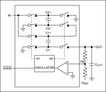
Figure 5. Internal components illustrate the operation of this regulated charge-pump inverter (MAX868).
The internal oscillator frequency (450kHz) is sufficiently high to ensure small external capacitors and high output current. Controlled by a comparator, the oscillator becomes active only when the output voltage is lower than its threshold. This regulation enables the circuit to provide constant output voltages as high as -2VIN. At the same time, the circuit draws minimum quiescent currents at light loads.
Another problem common in battery-powered applications is a battery voltage that ranges above and below the regulated output voltage. The output voltage of a Li+ cell varies from 3.6V to 1.5V during its lifetime, before it is recharged. To derive a constant 3.3V from this changing input, a combined buck/boost converter is required. Initially this device downconverts the full battery voltage (3.6V) to 3.3V. When the battery voltage drops below 3.3V, the step-up converter function guarantees the regulated 3.3V output voltage.
Though usually complicated, this approach can now be implemented with a simple charge-pump IC like the MAX1759. Operating from input voltages ranging from 1.6V to 5.5V, the MAX1759 generates an output either fixed (3.3V) or adjustable (2.5V to 5.5V) and delivers output currents up to 100mA. This IC comes in a 10-pin µMAX® package and operates with three external capacitors. An additional shutdown mode disconnects output from input while lowering the quiescent current to 1µA.
Tables 1 and 2 list some of the regulated and unregulated charge pumps available from Maxim, including those with special functions and all those mentioned in the text. These tables enable designers to choose a suitable charge pump according to the application's required package, functions, and output-current specifications.
Maxim continually introduces new products. We encourage you to browse Maxim's product lines for the most updated list of charge-pump devices. Capacitor charge pumps are shown under the Power and Battery Management category.
Table 1. Unregulated Charge Pumps
| Part Number | Input Voltage | Output Voltage | Output Current | Switching Frequency | Features |
| MAX828/MAX829 | 1.5V to 5.5V | -VIN | 25mA | 12kHz/35kHz | Inverter; 5-pin SOT23 package |
| MAX1720 | 1.5V to 5.5V | -VIN | 25mA | 12kHz | Inverter; low quiescent current, shutdown, 6-pin SOT23 package |
| MAX1719/1721 | 1.5V to 5.5V | -VIN | 25mA | 125kHz | Inverter; 6-pin SOT23 package, shutdown |
| MAX870/871 | 1.4V to 5.5V | -VIN | 25mA | 125kHz/500kHz | Inverter; 5-pin SOT23 package |
| MAX1682/1683 | 2V to 5.5V | 2 × VIN | 30mA | 12kHz/35kHz | Doubler; 5-pin SOT23 package |
| ICL7660 MAX1044 | 1.5V to 10V | -VIN, 2 × VIN | 10mA | 10kHz | Doubler or inverter; DIP, 8-pin SO |
| MAX860 | 1.5V to 5.5V | -VIN, 2 × VIN | 50mA | 6kHz; 50kHz; 130kHz | Doubler or inverter; 8-pin SO/µMAX |
| MAX861 | 1.5V to 5.5V | -VIN, 2 × VIN | 50mA | 13kHz; 100kHz; 250kHz | Doubler or inverter; 8-pin SO/µMAX |
| MAX1680 | 2V to 5.5V | -VIN, 2 × VIN | 125mA | 125kHz; 250kHz | Doubler or inverter; 8-pin SO/µMAX |
| MAX1681 | 3V to 5.5V | -VIN, 2 × VIN | 125mA | 500kHz; 1MHz | Doubler or inverter; 8-pin SO/µMAX |
| Part Number | Input Voltage | Output Voltage | Output Current | Switching Frequency | Features |
| MAX619 | 2V to 3.6V | +5V | 50mA | 500kHz | Regulated 5V, 8-pin SO package |
| MAX682 | 2.7V to 5.5V | +5V | 250mA | 50kHz to 2MHz | Regulated 5V, 8-pin SO/µMAX packages |
| MAX683 | 2.7V to 5.5V | +5V | 100mA | 50kHz to 2MHz | Regulated 5V, 8-pin SO/µMAX packages |
| MAX684 | 2.7V to 5.5V | +5V | 50mA | 50kHz to 2MHz | Regulated 5V, 8-pin SO/µMAX packages |
| MAX868 | 1.8V to 5.5V | Up to -2 × VIN | 30mA | up to 450kHz | Variable inverted voltage; µMAX package |
| MAX1673 | 2.0V to 5.5V | Up to -VIN | 125mA | 350kHz | Variable inverted voltage; fixed frequency |
| MAX1759 | 1.6V to 5.5V | 2.5V to 5.5V | 100mA | 1.5MHz | Buck/boost converter |
*博客内容为网友个人发布,仅代表博主个人观点,如有侵权请联系工作人员删除。