Battery Backup with Delay(具有时滞的备用电池)
Abstract: This application note explains that the simplest link from a main supply and backup battery to a load is the diode-OR connection. However simple that concept, a diode-OR does not work when the battery voltage exceeds the main supply voltage. The article presents a circuit which handles that condition. The MAX931 comparator with 2% reference is featured in the design.
This design idea appeared in the May 25, 2006 issue of Electronic Design magazine.
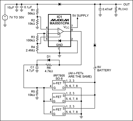
The simplest link from a main supply and backup battery to a load is the diode-OR connection. However, a diode-OR does not work when the battery voltage exceeds the main supply voltage. The Figure 1 circuit handles that condition. The main switch-mode supply voltage ranges from 7V to 30V, and the backup supply is a 9V battery.

Figure 1. IC1, the MAX931 comparator, monitors the main supply voltage. It also turns on the backup battery by grounding its negative terminal when the main supply drops below 7.4V.
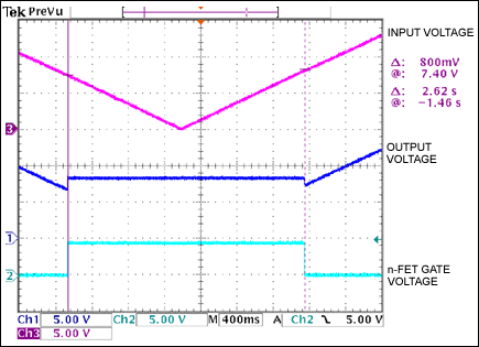
The MAX931 is an ultra-low-power comparator with a 1.182V bandgap reference. During normal operation the comparator output is low, the three parallel-connected n-channel FETs are off, and the battery's negative terminal floats. Power flows from the main supply to the load. When the main voltage declines to 7.4V the comparator's output goes high, turning on the n-FETs and grounding the negative terminal of the battery. Power then flows from the battery to the load (Figure 2).

Figure 2. In response to a gradual decrease in the main supply voltage (channel 3 in Figure 1), the n-FET gate voltage goes high (channel 2). This activates the battery and drives the output voltage (channel 1) to 9V. As the main supply voltages passes 8.4V the n-FETs turn off, allowing the output to resume tracking the main supply voltage.
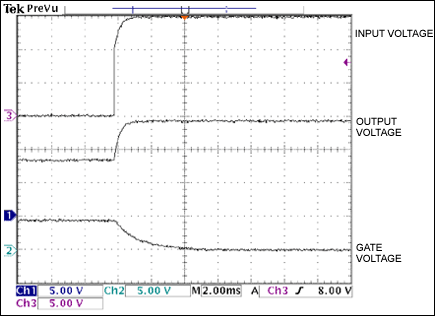
D1, C1, and R6 introduce a delay in the gate drive. This delay eliminates a supply-rail glitch that would otherwise occur when switching from the battery to the main supply. While those glitches can cause an unacceptable reset in the system's microcontroller, Figure 3 illustrates the absence of that effect with this circuit. Note that R3 and R4 set the hysteresis in the MAX931 to 800mV, as required for proper operation. See the MAX931 data sheet for calculation of those resistor values.

Figure 3. The output in Figure 1 responds without glitches in response to a fast restoration of the main supply voltage.
*博客内容为网友个人发布,仅代表博主个人观点,如有侵权请联系工作人员删除。